The MPM3695 Family: High-Power Module Solutions

Meeting High-Current and Precision Requirements
Powering modern applications requires high currents, precise transient control, and a flexible voltage set-up. In particular, field-programmable gate array (FPGA) power specifications often come with rigid requirements regarding output voltage (VOUT) accuracy, where the absolute VOUT accuracy must be around ±1.5%, regardless of temperature variations and aging. Some manufacturers’ load regulation specifications may be significantly more stringent. The most commonly used method to configure VOUT is to use external or internal voltage dividers. This method provides flexibility for VOUT configuration while fulfilling demanding requirements.
Flexible Power with the MPM3695 Series
The MPM3695 family (MPM3695-10, MPM3695-20, MPM3695-25, and MPM3695-100) was introduced to deliver up to 800A of current with ultra-fast transient response and excellent voltage tolerance. Depending on the application, designers can use either external or internal voltage dividers to provide excellent flexibility. The internal resistor divider offers compactness, integration, and ease of use. These features make the device suitable for designs with stringent space and performance requirements; meanwhile, the external resistor dividers provide flexibility, customization, and improved thermal management.
Introduction to High-Current, High-Efficiency Power Solutions
In recent years, fast-paced advancements in technology have required power supplies with higher output current (IOUT) capabilities. Unfortunately, delivering a significant IOUT with high efficiency in a compact package is a complex task for modern design solutions.
The MPM3695 family is a fully integrated power module solution with a PMBus interface that features paralleled connections, delivering outstanding IOUT delivery capabilities of up to 800A (see Table 1). MPS’s proprietary, multi-phase constant-on-time (MCOT) control provides ultra-fast transient response and simple loop compensation.
The PMBus interface enables simple module configuration and monitoring of key parameters, while the comprehensive protections ensure reliable operation. The MPM3695 can easily set VOUT margins, fault levels, and power good (PG) thresholds relative to VOUT. This flexibility allows for dynamic adjustments as VOUT changes, eliminating the need for manual updates and accelerating the design process.
Table 1: MPM3695 FamilySetting the Output Voltage
The MPM3695 family offers two possible methods to adjust VOUT. The first option is to use the internal resistor voltage divider. The second option is to change VOUT via the external resistor divider.
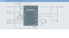
Figure 1 shows the typical application circuit with an internal resistor divider.
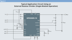
Figure 2 shows the typical application circuit with an external resistor divider.
Based on the design, it can be advantageous to utilize both methods for space-constrained applications with customization requirements. External resistor dividers can also improve thermal management, since the power dissipation can be spread across the PCB. However, one significant drawback of external resistors is that their tolerance can compromise VOUT accuracy. Furthermore, resistor dividers have a temperature coefficient, which means their resistance can fluctuate with changes in temperature. This variation can lead to slight deviations in the feedback voltage (VFB) and, consequently, VOUT.
The MPM3695 family supports the PMBus protocol for the VOUT configurations.
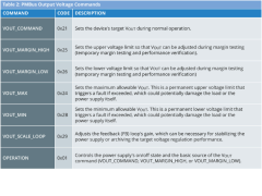
Table 2 shows the commands that can be used to change VOUT.
The margin voltage commands verify the application’s robustness and ensure that the device meets the application’s specifications and can tolerate small changes in power supply voltages across time and temperature changes.
Once the selected voltage value is determined, it is compared to the VOUT limits set by the VOUT_MAX and VOUT_MIN commands. This ensures that VOUT remains within safe upper and lower thresholds. Finally, a scaling factor is applied to match a reference voltage.
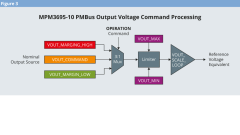
Figure 3: The VOUT command process for the MPM3695-10 involves using the OPERATION command to select one of the three inputs as the source of the nominal voltage (VOUT_COMMAND, VOUT_MARGIN_HIGH, or VOUT_MARGIN_LOW).
Internal Voltage Divider
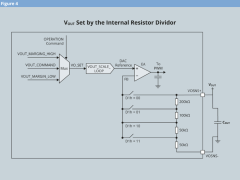
VOUT is sensed through the VOSNS+ and VOSNS- pins. The internal resistor divider reduces VOUT to match the reference voltage (VREF).
Figure 4 shows how to configure the internal voltage divider.
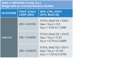
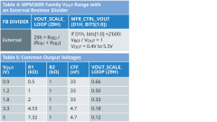
Table 3 shows the VOUT range using the internal voltage divider option through VOUT_SCALE_LOOP (29h) and MFR_CTRL_VOUT (D1h).
While using the internal voltage divider, it is important to completely disconnect the external feedback (FB) resistors and select the appropriate voltage range according to the desired application.
A higher FB gain typically leads to faster response times to load transients. However, excessively high gains can introduce instability or overshoot. A lower FB gain can lead to slower settling times and reduced overshoot.
External Voltage Divider
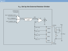
When using an external voltage divider, the device’s VOUT is scaled using two resistors (R1 and R2) connected in series to form a voltage divider configuration. VFB is sensed through the VOSNS+ and VOSNS- pins.
Figure 5 shows an external voltage divider configuration.
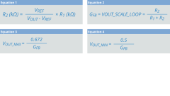
The values of the FB resistors (R2 and R1) can be calculated with Equation 1.
Where VREF is the reference voltage, which has a default value of 0.6V (and can be adjusted to be between 0.5V and 0.672V); and VOUT is the target output voltage.
It is recommended to use 1% tolerance resistors with a low temperature coefficient for the FB divider. The VOUT FB gain can be estimated with Equation 2.
For a given FB resistor network, the upper (VOUT_MAX) and lower limits (VOUT_MIN) of VOUT can be calculated with Equation 3 and Equation 4, respectively.
To optimize the load transient response, a feed-forward capacitor (CFF) must be placed in parallel with R1 (see Figure 5).
Table 4 shows the VOUT range when using the external voltage divider through VOUT_SCALE_LOOP (29h) and MFR_CTRL_VOUT (D1h).
Table 5 lists the values of the FB resistors and the feed-forward capacitor for common output voltages.
Practical Design Example
External Voltage Divider
The following section gives a practical example on how to set VOUT through the external resistor voltage divider using the MPM3695-25.
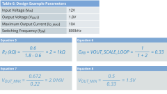
Table 6 shows all parameters considered for this example.
Choose R1 = 2kΩ and VREF = 0.6V. Estimate R2 with Equation 5.
Calculate the resistor divider gain with Equation 6.
VOUT_MAX and VOUT_MIN can be estimated with Equation 7 and Equation 8, respectively.
When using the resistor divider described above, failure to adhere to these limits reduces VOUT accuracy.
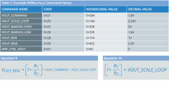
Table 7 shows the configuration values for the nominal VOUT command (VOUT_COMMAND) and the gain of the external resistor divider (VOUT_SCALE_LOOP) used in this example. It also includes the margin VOUT limit commands (VOUT_MARGIN_HIGH and VOUT_MARGIN_LOW) and the safeguard VOUT limit command (VOUT_MAX and VOUT_MIM) values.
The real output voltage (VOUT_REAL) can be calculated with Equation 9.
VOUT_REAL = VOUT_COMMAND if the following condition is satisfied, estimated with Equation 10.
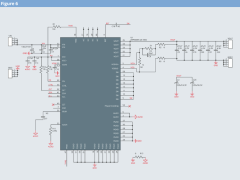
In our current example, VOUT_SCALE_LOOP matches the resistor divider’s real gain, so VOUT_REAL is equal to the value configured via VOUT_COMMAND (21h).The MPM3695-25's evaluation board (EVM3695-25-RF-02A) in a single-phase configuration was used for this example.
Figure 6 shows the circuit that was built.
MPS’s Virtual Bench Pro 4.0 GUI provides an interface to configure the MPM3695 family.
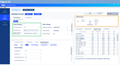
Figure 7 shows the main PMBus VOUT commands used in this example.
The “Parameters” tab is divided into two sections. The basic parameters are found at the top, while more advanced configurations are at the bottom. Box 1 in Figure 7 shows the configurations for VOUT_COMMAND (21h), VOUT_SCALE_LOOP (29h), and MRF_CTRL_VOUT (D1h). Box 2 in Figure 7 shows the following VOUT commands: VOUT_MAX (24h), VOUT_MIN (2Bh), VOUT_MARGIN_LOW (26h), and VOUT_MARGIN_HIGH (25h). The configuration value (in hexadecimal format) for each of these registers can be found in the “Register Map” tab in Box 3 (see Figure 7).
The MPM3695 family of power modules have telemetry commands such as READ_VIN (88h), READ_VOUT (8Bh), READ_IOUT (8Ch), and READ_TEMPERATURE (8Dh). These commands monitor the input voltage (VIN), VOUT, load current, and temperature in real time, respectively. The values are visualized in the “Monitoring” section in Box 4 (see Figure 7).
VOUT_COMMAND (21h) sets the nominal voltage source.
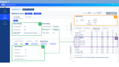
Figure 8 shows whether the values monitored in real time (indicated in the yellow box) match the target values from the application.
To set VOUT_MARGIN_HIGH (25h) as the nominal VOUT source and turn on the device with a high margin, set OPERATION (01h), bits[5:4] = 10b. Based on Table 6, the target margin high value is set to 2V.
Figure 8 shows whether VOUT as monitored in real time (indicated in the green box) matches the value configured via VOUT_MARGIN_HIGH (25h).
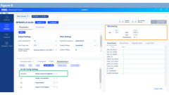
Figure 9 shows whether the result from VOUT_MARGIN_LOW (26h) matches the configured values used in this example.
Internal Voltage Divider
Consider the parameters in Table 6.
This section describes how to configure VOUT using the internal voltage divider.
Verify that the VOSNS+ and VOSNS- pins are connected directly to the VOUT sense points (see figure 4).
In this scenario, R3 is set to 0Ω, and R4 was removed in Figure 6.
For safety considerations while switching between internal and external dividers, it is highly recommended to disable the part through the EN pin; otherwise, the device could sustain damage. The VOUT range was set via MFR_CTRL_VOUT (D1h), bits[1:0] (when set to 10b), and VOUT_SCALE_LOOP (29h) was set to 0x00FA (see Table 3).
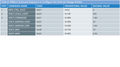
Table 8 shows the PMBus command sequence to set VOUT to 1.8V using the internal resistor divider.
Adjusting VOUT on-the-fly via the PMBus interface is particularly useful when changing the I/O voltage, such as when reconfiguring the functionality of new FPGAs like the Achronix Speedster7t solution. Additionally, this on-the-fly feature can also be utilized to adjust the FPGA’s core voltage during operation to minimize power consumption.
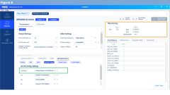
Figure 10 shows the GUI when configuring VOUT with the internal resistor divider, where the green box shows the commanded values for VOUT_COMMAND (21h) and MFR_CTRL_VOUT (D1h), bits[1:0]. The VOUT current measurement, load current, and device’s temperature can be monitored in the “Monitoring” section (indicated in the yellow box) (see Figure 10).
Conclusion
Choosing between an internal or external voltage divider to configure VOUT depends on the specific requirements of the application, including design flexibility, space constraints, precision needs, and susceptibility to environmental factors.
The MPM3695 family (MPM3695-10, MPM3695-20, MPM3695-25, and MPM3695-100) offers excellent flexibility to configure VOUT by using either an external or internal voltage divider. Based on the results presented, both methods provide high accuracy for real-time VOUT measurements. Furthermore, by including the margin levels and PMBus commands, the MPM3695 family is well-suited for applications where precise VOUT control is needed.
Your Contact Person
Thomas Merkel is ready to assist you with further information about the MPM3695 Family.
